DIGITAL LOGIC FAMILY
The basic Classification of the Logic Families are as follows:
A) Bipolar Families
B) MOS Families
C) Hybrid Devices
A) Bipolar Families:
1. Diode Logic (DL)
2. Resistor Transistor Logic (RTL)
3. Diode Transistor Logic (DTL)
4. Transistor- Transistor Logic (TTL)
5. Emitter Coupled Logic (ECL) or Current Mode Logic (CML)
6. Integrated Injection Logic (IIL)
B) MOS Families:
1. P-MOS Family
2. N-MOS Family
3. Complementary-MOS Family
• Standard C-MOS
• Clocked C-MOS
• Bi-CMOS
• Pseudo N-MOS
• C-MOS Domino Logic
• Pass Transistor Logic
C) Hybrid Family:
Bi-CMOS Family
CMOS Family TTL Family
WHAT IS LOGIC FAMILY
Logic families are groups of logic circuits that are based on particular types of elements (resistors, transistors, and so forth). Families are identified by the manner in which the elements are connected, and, in some cases, by the types of elements used.
CMOS v/s TTL
There are two different types of computer chips: CMOS and TTL. CMOS stands for complementary metal-oxide-semiconductor. TTL stands for transistor-transistor logic. They’re both oftentimes used to make microchips. However, they’re both different and serve different functions. To learn more about the difference between CMOS and TTL, we must understand its functioning.
The difference between CMOS and TTL is that CMOS (complementary metal-oxide-semiconductor) is an electronic component in the logic family. CMOS is used in computers and various other electronic devices. TTL (transistor-transistor logic) is a type of digital logic in the logic family. TTL is also used in computers and various other electronic devices.
CMOS, Or complementary metal oxide semiconductor, uses PMOS and NMOS types of field-effect transistors to handle input and output. They are commonly used in NAND and NOR gates and are economically efficient, and have a higher clock rate making them consume more power than TTL or transistor-transistor logic units.
TTL and Transistor-Transistor Logic Units are made up of BJTs Or bipolar junction transistors that commonly have multiple inputs and outputs. They have a slightly lower density of logic gates and usually are found with NAND gates. However, they consume less power and hence are used in several devices.
Types of Gates
The different types of logic gates and symbols with truth tables are discussed below.
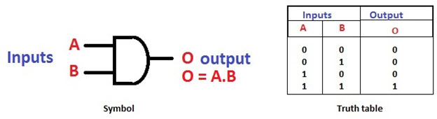
AND Gate
The AND gate is a digital logic gate with ‘n’ i/ps one o/p, which performs logical conjunction based on the combinations of its inputs. The output of this gate is true only when all the inputs are true. When one or more inputs of the AND gate’s i/ps are false, then only the output of the AND gate is false. The symbol and truth table of an AND gate with two inputs is shown below.
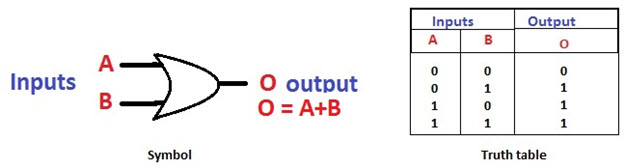
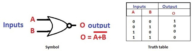
OR Gate
The OR gate is a digital logic gate with ‘n’ i/ps and one o/p, that performs logical conjunction based on the combinations of its inputs. The output of the OR gate is true only when one or more inputs are true. If all the i/ps of the gate are false, then only the output of the OR gate is false. The symbol and truth table of an OR gate with two inputs is shown below.
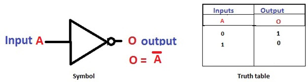
NOT Gate
The NOT gate is a digital logic gate with one input and one output that operates an inverter operation of the input. The output of the NOT gate is the reverse of the input. When the input of the NOT gate is true then the output will be false and vice versa. The symbol and truth table of a NOT gate with one input is shown below. By using this gate, we can implement NOR and NAND gates.
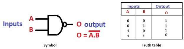
NAND Gate
The NAND gate is a digital logic gate with ‘n’ i/ps and one o/p, that performs the operation of the AND gate followed by the operation of the NOT gate.NAND gate is designed by combining the AND and NOT gates. If the input of the NAND gate high, then the output of the gate will be low.The symbol and truth table of the NAND gate with two inputs is shown below.
NOR Gate
The NOR gate is a digital logic gate with n inputs and one output, that performs the operation of the OR gate followed by the NOT gate. NOR gate is designed by combining the OR and NOT gate. When any one of the i/ps of the NOR gate is true, then the output of the NOR gate will be false. The symbol and truth table of the NOR gate with the truth table is shown below.
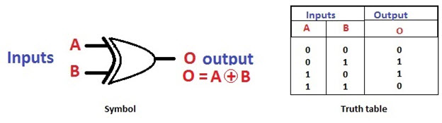
Exclusive-OR Gate
The Exclusive-OR gate is a digital logic gate with two inputs and one output. The short form of this gate is Ex-OR. It performs based on the operation of the OR gate. . If any one of the inputs of this gate is high, then the output of the EX-OR gate will be high. The symbol and truth table of the EX-OR are shown below.
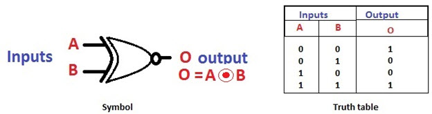
Exclusive-NOR Gate
The Exclusive-NOR gate is a digital logic gate with two inputs and one output. The short form of this gate is Ex-NOR. It performs based on the operation of the NOR gate. When both the inputs of this gate are high, then the output of the EX-NOR gate will be high. But, if any one of the inputs is high (but not both), then the output will be low. The symbol and truth table of the EX-NOR are shown below.
IC Packaging
2. Provides a completed unit large enough to handle.
3. So that it is large enough for electrical connections to be made.
4. Material is molded plastic, epoxy, resin, or silicone. Ceramic used if higher thermal dissipation capabilities required. Metal/glass used in special cases.
Three most common packages for ICs are
a) dual-in-line (DIPS) (most common)
b) flat pack
c) axial lead (TO5)

Characteristics of Digital ICs
Input /Output voltage level:
The following currents and voltages are specified which are very useful in the design of digital systems.
High-level input voltage, VIH : This is the minimum input voltage which is recognized by the gate as logic 1.
Low-level input voltage, VIL: This is the maximum input voltage which is recognized by the gate as logic 0.
High-level output voltage, VOH: This is the minimum voltage available at the output corresponding to logic 1.
Low-level output voltage, VOL: This is the maximum voltage available at the output corresponding to logic 0.
High-level input current, IIH : This is the minimum current which must be supplied by a driving source corresponding to 1 level voltage.
Low-level input current, IIL: This is the minimum current which must be supplied by a driving source corresponding to 0 level voltage.
High-level output current, IOH: This is the maximum current which the gate can sink in 1 level.
Low-level output current, IOL: This is the maximum current which the gate can sink in 0 level.
High-level supply current, ICC (1): This is the supply current when the output of the gate is at logic 1.
Low-level supply current, ICC (0): This is the supply current when the output of the gate is at logic (0).
Propagation Delay:
Definition: The time required for the output of a digital circuit to change states after a change at one or more of its inputs. The speed of a digital circuit is specified in terms of the propagation delay time. The delay times are measured between the 50 percent voltage levels of input and output waveforms. There are two delay times, tpHL: when the output goes from the HIGH state to the LOW state and tpLH, corresponding to the output making a transition from the LOW state to the HIGH state. The propagation delay time of the logic gate is taken as the average of these two delay times.
Fan-in
Defination: Fan-in (input load factor is the number of input signals that can be connected to a gate without causing it to operate outside its intended operating range. expressed in terms of standard inputs or units loads (ULs).
Fan-out
Defination:Fan-out (output load factor) is the maximum number of inputs that can be driven by a logic gate. A fanout of 10 means that 10 unit loads can be driven by the gate while still maintaining the output voltage within specifications for logic levels 0 and 1.
Digital IC gates are classified not only by their logic operation, but also by the specific logic circuit family to which it belongs. Each logic family has its own basic electronic circuit upon which more complex digital circuits and functions are developed.
Different types of logic gate families :
RTL : Resistor Transistor Logic gate family
DCTL : Direct Coupled Transistor Logic gate family
RCTL : Resistor Capacitor Transistor Logic gate family
DTL : Diode Transistor Logic gate family
TTL : Transistor Transistor logic gate family
IIL : Integraeted Injection gate family
TTL Logic family
The evolution from Diode transistor Logic to transistor transistor Logic can be seen by observing the placement of p-n junctions. For example, the diode in the DTL can be replaced by a transistor whose collector is pulled up to the power supply. The p-n junction of diode is replaced by the BE junction of transistor and with the current gain of the transistor, the current going into the base of transistor is greatly increased, increasing the fanout. The input diodes are replaced by the multi-emitter NPN transistor. Later on, we will make additional modifications to this circuit to improve its performance further. The analysis of this circuit follows very much the same path as the analysis of the DTL gate. For the most part, we will consider the input transistor, act just like two diodes.
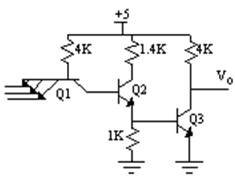
TTL inputs: multiple-emitter
A two input standard TTL NAND gate is a multiple emitter transistor for the inputs A and B. the output transistors Q3 and Q4 form a totem-pole output arrangement.
Operation:
If A or B is low, the base-emitter junction of Q1 is forward biased and its base-collector junction is reverse biased. Then there is a current from Vcc through R1 ti the base emitter junction of Q1 and into the LOW input, which provides a path to the ground for the current. Hence there is no current into the base of Q2 and making it into cur-off. The collector of Q2 is HIGH and turns Q3 into saturation. Since Q3 acts as a emitter follower, by providing a low impedance path from Vcc to the output, making the output into HIGH. At the same time, the emitter of Q2 is at ground potential, keeping Q4 OFF.
When A and B are high, the two input base emitter junctions of Q1 are reverse biased and its base collector junction is forward biased. This permits current through R1 and the base collector junction of Q1 into the base of Q2, thus driving Q2 into saturation. As a result Q4 is turned ON by Q2, and producing LOW output which is near ground potential. At the same time, the collector of Q2 is sufficiently at LOW voltage level to keep Q3 OFF.
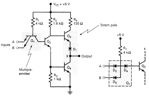
TTL outputs: Totem pole/ active pull-up
It is possible in TTL gates the charging of output capacitance without corresponding increase in power dissipation with the help of an output circuit arrangement referred to as an active pull-up or totem-pole output. In this case,
• Outputs must never be connected together.
• Connecting outputs causes excessively high currents to flow.
• Outputs will eventually be damaged.
• The standard TTL output configuration with a HIGH output and a LOW output transistor, only one of which is active at any time.
• A phase splitter transistor controls which transistor is active.
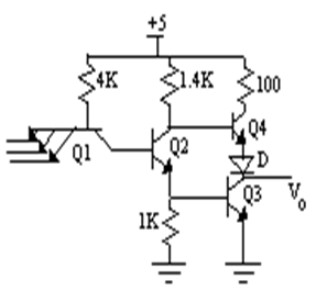
One of the problems with the TTL gate circuit is that the pull-up resistor on the output transistor will prevent rapid charging of any wiring capacitance on the output. One way to improve the rise time is to reduce the resistance value as is often done, but this also increases the power dissipation when the output is low. If we look at the circuit, we observe that when the transistor is saturated, it presents a very low effective resistance to ground. The problem arises when the output is high and the pull-up resistor is too large. Ideally we would like to have a very low resistance pull-up when the output is high, but a very high pull-up resistance when the output is low. In this way, we could get quick charging and very low power dissipation. The totem-pole output stage for TTL, shown in Figure .
The TTL family includes,
standard TTL designed as 74 or 54
low-power TTL designed as 74L or 54L
high-power TTL designed as 74H or 54H
low-power Schottky TTL designed as 74LS or 54LS
Schottky TTL designed as 74S or 54S
advanced low-power Schottky TTL designed as 74ALS or 54ALS
advanced Schottky TTL designed as 74AS or 54AS
Fast TTL designed as 74F or 54F
An alphabetic code preceding this indicates the name of the manufacturer. A two-, three- or four-digit numerical code indicates the logic function performed by the IC.
Comments
Post a Comment